Years ago I made several prototypes of controllers and actuators. Here are described the first experiments and technologies used. From the first rough initial attempts, until a first suite of devices based on Microcontrollers.
The first experiments were based on PC. I used that in the mid-90s were more ports available and frequently used in a PC.
- The parallel port (IEEE 1284 DB 25 Female Connector)
- The Serial port (RS232C DB 9 or DB 25 Male Connector)
Initially I started to use the parallel port. I started to work with the parallel port for ease of use and for my purpose, which required what today would be called GPIO.
PC based studio
In an old style PC equipped with parallel port its mode of operation could be set via BIOS to Unidirectional, Bidirectional, EPP, and ECP. The parallel port was conceived and subsequently specialized for printers, but it was also used for Scanners and External Drivers such as the Iomega Zip drive.
For this reason, to make a customized use for DIY ![]() you have to write a device driver for your specific device. In addition to a modern operating system, just a process in kernel mode has access to locations (legacy) of the registers of the parallel port. LPT1 (0x3BC) to LPT2 (0×378) or LPT3 (0×278).
you have to write a device driver for your specific device. In addition to a modern operating system, just a process in kernel mode has access to locations (legacy) of the registers of the parallel port. LPT1 (0x3BC) to LPT2 (0×378) or LPT3 (0×278).
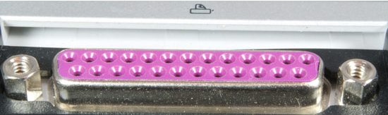
pin function
 2   D0
 3   D1
 4   D2
 5   D3
 6   D4
 7   D5
 8   D6
 9   D7
Pins 18,19,20,21,22,23,24 and 25 are all ground pins.
Here then find the complete pinout: Parallel Port complete Pinout. Since I wanted to use all eight data pins, I chose the port operation mode in Unidirectional and Bidirectional (Byte Mode).
PC parallel port can be very useful I/O channel for connecting your own circuits to PC. The PC’s parallel port can be used to perform some very amusing hardware interfacing experiments. The port is very easy to use when you first understand some basic tricks.
WARNING: PC parallel port can be damaged quite easily if you make mistakes in the circuits you connect to it.
Those datapins are TTL level output pins. This means that they put out ideally 0V when they are in low logic level (0) and +5V when they are in high logic level (1). In real world the voltages can be something different from ideal when the circuit is loaded. The output current capacity of the parallel port is limited to only few milliamperes.
Here is a simple idea how you can connect load to a PC parallel port data pins.
        Dn Out ------+
                     |+
  Sourcing         Load (up to 2.6 mA @ 2.4 v)
                     |-
        Ground ------+
This is not the only way to connect things to a parallel port.
The parallel port data pins are TTL outputs, that can both sink and source current. In ordinary parallel port implementations the data outputs are 74LS374 IC totem-pole TTL outputs which can source 2.6 mA and sink 24 mA.
Regular TTL outputs basically consist of a two “stacked” transistor in series between +5 volts and ground, with the output coming from the connection between them. This is called a “totem pole output”. At any given time one of these transistors is conducting and the other is not. To pull the output “high”, the transistor from +5 to the output conducts (H), which “sources” positive current from the output to ground (that is, an external device between the output and ground will get power). To pull the output low, only the lower transistor (L) conducts, “sinking” current to ground; an external device between +5 volts and the output can be energized.
         +5
        /    |
    ---H on  V
        \      -->
         |________        TTL output on = 1 = high, "sourcing" current
         |   out  \
        /         / |
    ---L off      \ V
        \_________/
        Gnd

       +5_________
        /         \
    ---H off      / |
        \         \ V
         |________/      TTL output off = 0 = low, "sinking" current
         |  <-- out
        /
    ---L on |
        \   V
        Gnd
The outputs are designed so that they give at least 2.4V at 2.6 mA load. This 2.6 mA figure is for ordinary LS-TLL circuits used, the LSI implementations used in many computers can give more or less. For example quite popular (few years ago) UM82C11-C parallel port chip can only source 2 mA.
Simple current sourcing load connection:
        Dn Out ------+
                     |+
  Sourcing         Load (up to 2.6 mA @ 2.4 v)
                     |-
        Ground ------+
When taking current from PC parallel port, keep the load low, only up to few milliamperes. Trying to toke too much current (for example shorting pins to ground) can fry the parallel port. I have not killed any parallel port (yet) in this method, but I have had in cases where too much load has made the parallel port IC very hot. Be careful.
If you have an external +5 volt supply, you have another option for connection: use the Data Out pins to sink up to 24 mA from your +5 volt supply. This can be made with a circuit like this:
                     +------------------------------- (+5 v)
                     |+
   Sinking         Load (up to 24 mA @ 4.2v)
                     |-	     Power Supply
        Dn Out ------+

        Ground -------------------------------------- ( Gnd)
The load gets power then you have external +5V on and the printer port data pin set to 0. This circuit gives you capability of of driving more current than the “sinking” approach. You need to be careful with this circuit, because with this circuit you can easily fry the parallel port if you do things wrong. My advice is to be very careful with this type of circuit and make sure that the external +5V power supply gets turned off when computer gets turned off (all printer ports might not like getting +5V though the load to printer port when they are not powere). The most convient source “external +5V” might be from same other port on your PC (USB, joystick, keyboard/mouse etc. port).
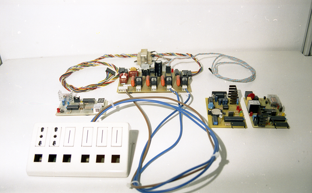
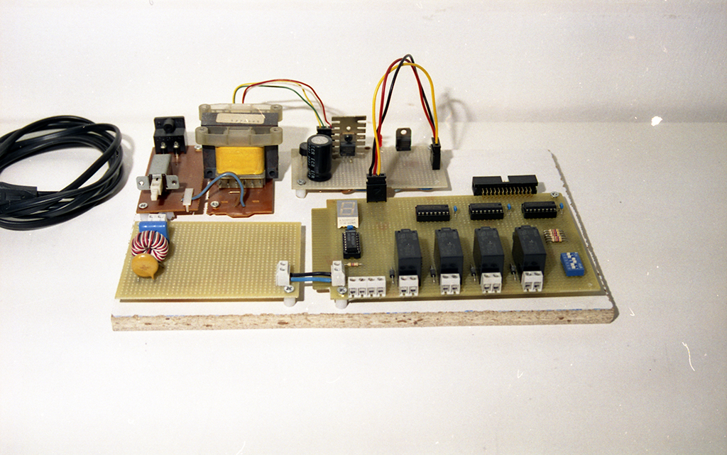
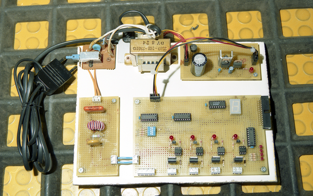
I have used mostly “sinking” type circuits. On this proto-card I made my first experiments.
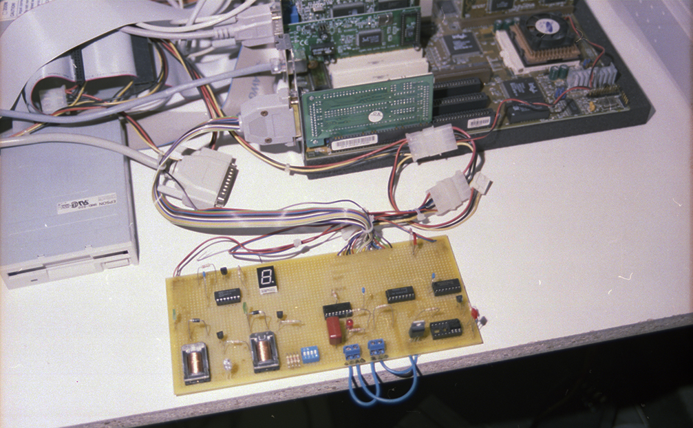
This card initially was driving the LEDs only. ![]() After I refined the code to use a decoder BCD 7-segment with its display. Then I was able to drive a relay, and finally a TRIAC power On / Off mode. I admit I blew an optocoupler for triac faulty.
After I refined the code to use a decoder BCD 7-segment with its display. Then I was able to drive a relay, and finally a TRIAC power On / Off mode. I admit I blew an optocoupler for triac faulty. ![]()
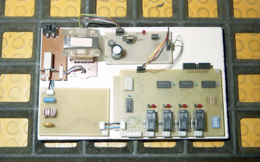
This is my first final with implemetazione Power Relay (up to 1KW). I had called Smart Switch 100. I also made for Windows 3.x, Win95, Win98, WinME a DLL written in MS Visual C++, also provided a BAS file with the API definitions for use in MS Visual Basic widely used at the time. You can ask me the code if you’re interested.
The implementation of 16-bit is not required to create a device driver. Before NT 32-bit, Windows was based on MS-DOS kernel. In WinNT 3.x, 4 I had to work with the DDK and create a SYS driver to install and start in the operating system. In the NT version, the DLL becomes just a stub that calls the functions in the SS100 device driver.
Subsequent implementation of the SS100 in the solid state with the use of TRIAC power driven in On / Off mode. SS100 TRIAC was perfectly compatible and transparent to the code that could be used into both models.
 |
 |
| Return to home page Home Page | Continued on next Page 2 |